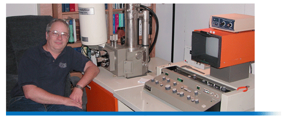
Lee Levine, Process Expert
Qualifications
Lee is an internationally recognized semiconductor assembly process expert with over 25 years of targeted experience in technical process development and optimization. He is known for keen analytical and troubleshooting skills in the creative and effective resolution of problems in production processes. He consistently produces business results that create enhanced revenue opportunities, higher yields and trouble free operations.
Experience
Previous experience includes 20 years as Principal and Staff Metallurgical Process Engineer at Kulicke & Soffa. and Distinguished member of the Technical Staff at Agere Systems. He was awarded 4 patents, published more than 50 technical papers, and won the 1999 John A. Wagnon Technical Achievement award from the International Microelectronics and Packaging Society (IMAPS). Major innovations include copper ball bonding, loop shapes for thin, small outline packages (TSOP and TSSOP, and CSPs) and introduction of DOE and statistical techniques for understanding assembly processes. He is a Fellow, V.P. of the Keystone Chapter, and V.P Technology for IMAPS.
Lee is a graduate of Lehigh University, Bethlehem, Pa where he earned a degree in Metallurgy and Materials Engineering.